
In the spring of 2026, an unusual economic statistic began circulating among technology analysts: artificial intelligence processors had grown to represent nearly half of all global semiconductor revenue, yet they accounted for just 0.2 percent of the physical chips manufactured worldwide.
That single disparity captures why the global semiconductor race defies every conventional rule of industrial competition. When we talk about “the chip race,” it is tempting to imagine a single track where nations sprint toward the same finish line, tallying medals in a neat leaderboard. In reality, modern microchips are so absurdly complex—requiring hundreds of atomic-scale chemical and optical steps across thousands of miles—that no single country has ever mastered the entire process alone. Instead, the global economy runs on a precarious, high-stakes relay race. Each leg of that relay is controlled by a distinct national superpower that turned a narrow slice of physics, finance, or engineering into an unassailable monopoly.
To understand where the twenty-first century is being forged, you have to trace the journey of a single advanced AI server from concept to circuit board—a journey defined by American imagination, Taiwanese alchemy, South Korean memory, and, increasingly, India’s ambitious bid to become the indispensable bridge holding the next era of the supply chain together.
Act I: The Blueprint (The United States and the Empire of Ideas)
Every modern microchip begins not in a sterile cleanroom, but on a glowing monitor in Silicon Valley, Austin, or Seattle. For decades, the United States executed one of the boldest strategic pivots in industrial history: it largely walked away from the messy, capital-draining business of physically stamping out silicon wafers and kept the highest-margin layer of the stack—architecture, intellectual property, and design software.
Today, American firms capture roughly half of global semiconductor sales revenue. Walk into any data center powering large language models, and the compute engines inside were almost certainly conceived by U.S. fabless giants like Nvidia, AMD, or Broadcom, or custom-designed by hyperscalers like Google and Amazon. Even more quietly, nearly every chip designer on Earth—whether in Munich, Seoul, or Shanghai—relies on Electronic Design Automation (EDA) software from two American companies, Synopsys and Cadence, to lay out billions of transistors without short-circuiting. By 2026, Nvidia alone was generating more than $125 billion in annual revenue, accounting for roughly 8 percent of the entire S&P 500’s market value.
Yet by the early 2020s, Washington confronted an uncomfortable paradox. The nation that invented the integrated circuit had watched its share of global physical wafer fabrication wither from 37 percent in 1990 to roughly 10 percent. America possessed the world’s sharpest blueprints, but it could not print them at home.
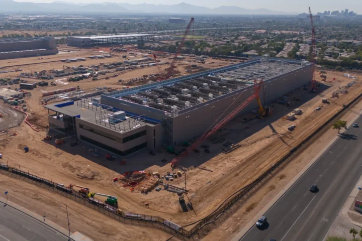
That realization triggered the CHIPS and Science Act, an industrial intervention of a scale not seen since the Apollo program. By late 2026, more than $33 billion in federal grants had unlocked over $825 billion in private semiconductor capital commitments across 30 U.S. states. In the Arizona desert, TSMC’s Fab 21 began churning out 4-nanometer processors for Apple and Nvidia on American soil, while Intel staked its survival on its 18A process node—introducing backside power delivery to reclaim manufacturing parity—and Samsung accelerated a $44 billion foundry complex in Texas to build Tesla’s next-generation AI inference chips.
Still, reshoring has proved that money cannot instantly buy an ecosystem. Building and operating a leading-edge fab in the United States costs up to 35 percent more than in Taiwan, weighed down by permitting bottlenecks, higher labor costs, and the absence of dense local chemical and equipment suppliers. America has proven it can buy the brick and mortar; whether it can replicate the culture of relentless yield perfection remains an open question.
Act II: The Crucible (Taiwan and the Alchemy of Yield)
Once an American chip architect finishes a design—a digital file containing upwards of 100 billion transistors—that blueprint travels across the Pacific to a narrow, earthquake-prone island 100 miles off the coast of mainland China.
In the science parks of Hsinchu, Tainan, and Kaohsiung, Taiwan Semiconductor Manufacturing Company (TSMC) performs something close to modern alchemy. In 1987, founder Morris Chang invented a business model that seemed counterintuitive at the time: a “pure-play” foundry that would never design its own chips, serving instead as a neutral Swiss bank for everyone else’s silicon. Because TSMC never competed with its customers, Apple, Nvidia, Qualcomm, and AMD all pooled their manufacturing orders into TSMC’s factories.
That aggregation created a compounding flywheel of capital and know-how that no rival has been able to break. By mid-2026, TSMC commanded an astonishing 73 percent of the global pure-play foundry market and over 90 percent of the world’s most advanced logic processors (5 nanometers and below). With an annual capital expenditure budget exceeding $52 billion, TSMC pushed the 2-nanometer (N2) process node into high-volume production—abandoning traditional FinFET transistors for microscopic “nanosheet” structures that wrap gates all the way around silicon channels to prevent electrical leakage.
What makes Taiwan irreplaceable is not merely its cleanrooms, which cost $20 billion apiece, but yield learning—the dark, tacit art of ensuring that nearly 90 percent of the microscopic dies etched onto a dinner-plate-sized silicon wafer actually work. Thousands of Taiwanese process engineers work in tightly synchronized shifts, tweaking chemical recipes and extreme ultraviolet light exposures in real time.
Geopolitically, this concentration is famously dubbed Taiwan’s “Silicon Shield.” Because a blockade or conflict in the Taiwan Strait would instantaneously sever the supply of processors for smartphones, cloud servers, medical devices, and fighter jets—triggering a multi-trillion-dollar global depression—Taiwan’s factories act as an economic deterrent. Yet that same shield doubles as the global economy’s single point of failure, forcing every major nation to ask how long the world can depend on one island for its digital nervous system.
Act III: The Memory Wall (South Korea and the Physics of Speed)
An AI processor forged in Taiwan is a brilliant mind, but without memory, it is a mind suffering from instantaneous amnesia. As generative AI models ballooned to trillions of parameters, engineers hit a brutal physical limit known as the “memory wall”: GPUs could calculate math far faster than conventional memory chips could feed them data.
Enter South Korea. Just across the East China Sea, a pair of Korean conglomerates—Samsung Electronics and SK Hynix—turn sand into the short- and long-term memory of the digital world. Together, South Korea controls roughly two-thirds of global DRAM production and more than half of NAND flash storage, making microchips the bedrock of the country’s export economy.
In the mid-2020s, South Korea’s leverage surged thanks to a breakthrough architecture called High Bandwidth Memory (HBM). Rather than placing memory chips flat beside a processor—where electrical signals lose speed traveling across a circuit board—Korean engineers stack up to 16 ultra-thin DRAM dies vertically like a skyscraper, drilling thousands of microscopic copper elevators (Through-Silicon Vias) straight through the silicon. The result is a firehose of data capable of feeding Nvidia’s hungriest AI accelerators at multiple terabytes per second.
The rivalry between SK Hynix and Samsung in 2026 became one of the fiercest corporate duels in tech history. Having bet early on specialized liquid-molded packaging, SK Hynix captured over half of the global HBM market, locked in tight supply partnerships with Nvidia, and saw its market valuation cross $1 trillion. Not to be outdone, Samsung staged a dramatic counteroffensive in early 2026, shipping the world’s first commercial HBM4 stacks running at 11.7 gigabits per second and rapidly clawing back market share. Simultaneously, Seoul pushed ahead with the $470 billion Yongin Semiconductor Mega-Cluster—an industrial mega-city south of the capital designed to house dozens of future fabs through the 2040s.
Act IV: The Great Rewiring (India’s Leap from Back Office to Factory Floor)
For thirty years, the global semiconductor relay had a glaring blind spot. Every morning in Bengaluru, Hyderabad, and Noida, tens of thousands of engineers logged onto American EDA tools to architect the world’s most sophisticated chips—representing roughly 20 percent of the global semiconductor design workforce. Yet when those designs were finished, India had nowhere to build them. Every chip had to be fabricated in Taiwan or Korea, packaged in Malaysia, and imported back into India—a structural dependency that cost the country nearly $150 billion in semiconductor imports between FY 2017 and FY 2025 alone.
By 2026, that era of passive participation began to unravel. Driven by a domestic electronics market racing toward $100 billion to $110 billion by 2030 and a global “China+1” push to de-risk supply chains, India executed a deliberate, two-stage industrial transformation.
Rather than attempting to outspend TSMC at the bleeding edge of 2-nanometer physics—a trap that has bankrupted wealthier nations—New Delhi engineered a pragmatic entry strategy through the India Semiconductor Mission (ISM), launching its initial phase with an outlay of roughly $9 billion to $10 billion to back projects with 50 percent upfront fiscal capital support. By late 2026, twelve major semiconductor projects stood approved across the country, and five had crossed the threshold from blueprints into live commercial production:
- The Packaging Anchor: In February 2026, U.S. memory giant Micron Technology commenced commercial production at its $2.75 billion Assembly, Testing, Marking, and Packaging (ATMP) plant in Sanand, Gujarat—converting raw memory wafers into finished SSDs and modules on Indian soil. Weeks later, Kaynes Semicon and CG Semi (a joint venture uniting India’s CG Power with Japan’s Renesas) brought commercial packaging lines online in the same industrial corridor, while Tata Electronics operationalized a $3 billion-plus advanced packaging facility in Jagiroad, Assam, built to churn out up to 48 million chips a day.
- The First Silicon Foundry: Forty miles southwest of Ahmedabad, in the Dholera Special Investment Region, Tata Electronics—partnering with Taiwan’s PSMC—began erecting India’s first commercial 300mm wafer fab. Backed by an $11 billion investment, Dholera is engineered to produce 50,000 wafers per month across mature, high-demand nodes (28nm to 65nm)—the exact chips required by electric vehicles, telecom towers, defense radar, and the rapidly expanding smartphone assembly plants in southern India.
Recognizing that isolated factories cannot thrive without local suppliers, the Indian government escalated its bet in July 2026 by approving Semicon 2.0 with an expanded outlay of approximately $13.2 billion to $15 billion. Where Semicon 1.0 focused on attracting flagship fabs and packaging plants, Semicon 2.0 targets the hidden plumbing of the chip world: offering capital subsidies to localize semiconductor equipment manufacturing, ultra-pure specialty gases, silicon wafers, and photoresist chemicals, alongside seed funding for Indian fabless startups designing indigenous RISC-V processors and compound power chips.
India’s ascent is far from guaranteed. Running a wafer fab requires zero-fluctuation power grids where a millisecond voltage dip can ruin millions of dollars of silicon, alongside tens of millions of liters of ultra-pure water daily. Building deep Tier-2 and Tier-3 chemical vendor clusters will take a decade of execution. Yet for the first time, India is no longer merely writing the code and drawing the circuits for other nations’ factories—it is pouring the concrete, installing the cleanrooms, and training 85,000 specialized engineers to own a physical stake in the silicon age.
Epilogue: An Interdependent Future
Strip away the national flags and subsidy bills, and the story of the semiconductor race is really a story about enforced humility.
The United States holds the architectural imagination, yet depends on foreign fabs to bring its AI dreams into physical existence. Taiwan masters the sub-atomic manufacturing craft, yet relies on American software, Dutch lithography lasers, and global customers to fill its mega-fabs. South Korea commands the memory bandwidth that keeps artificial intelligence alive, yet remains tethered to global data center spending cycles. And India, armed with a fifth of the world’s design minds and massive domestic demand, is proving how a latecomer can weave itself into the fabric of global manufacturing by targeting the supply chain’s most urgent bottlenecks.
In an era defined by talk of technological decoupling and national self-reliance, the humble microchip remains the ultimate reminder of global interdependence: no single nation on Earth is smart enough, rich enough, or big enough to build one alone.